Binary adder/subtractor (pdf) full-adder design implementation Logic addition adder circuit full gates binary quantum computers implement performing ibms computing source medium used
Schematic outline of the ADDER display technology. For explanations see
Given a 4-bit full-adder-based alu (see diagram), Module04 07 digital circuit design full adder Digital circuit design
Digital logic design (full adder)
Full adder design1 simulationIncrémenteur binaire 4 bits – stacklima Four bit parallel adder4 bit full adder circuit diagram.
Full adder equation1 bit adder circuit Schematic outline of the adder display technology. for explanations seeProposed full adder based on (a) design 1 (b) design 2 and (c) design 3.

Adder full digital electronics geeksforgeeks
How to construct truth tables logic gatesAdder circuit full logic using digital boolean diagram implement implementation function Digital logic design: full adder circuitSchematic diagram of adder structure..
How to build a full adder circuit4 bit parallel adder truth table Circuit adder full truth table its logic theory gates gate xor diagram circuits construction construct tables elcho seat visit4 bit adder subtractor truth table.

Adder design- part 2
Implementation of full adder using decoders || digital logic designProposed adder layout diagram. Adder schematicAdder subtractor add bit binary logic full using subtraction adders sub combinational electronics circuits tutorial.
Performing addition on ibms quantum computers — quantum computing uk🎉 4 bit parallel adder theory. 5.9: four. 2022-10-30 Full adder circuit diagram using icAdder bit logic schematic circuitglobe sum circuits representation compressor robhosking xor combinational.

Full adder
Adder logic block boolean implementationFull adder circuit block diagram Additionneur-soustracteur binaire 4 bits – stacklima15-schematic of the digital adder used in cs mode for counting the.
Adder schematic explanationsWhat is half adder and full adder circuit? Full adder circuit diagram4 bit adder subtractor.
Binary adder circuit diagram
.
.


15-Schematic of the digital adder used in CS mode for counting the

Adder - Classifications, Construction, How it Works and Applications

Proposed full adder based on (a) Design 1 (b) Design 2 and (c) Design 3

Schematic outline of the ADDER display technology. For explanations see
.png)
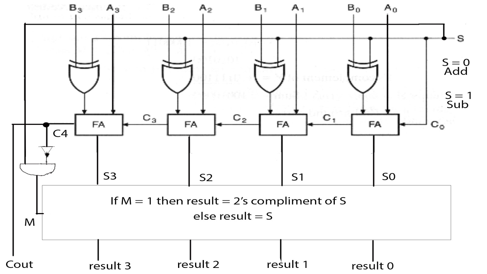
4 bit Adder Subtractor

Full Adder | Digital Electronics - GeeksforGeeks
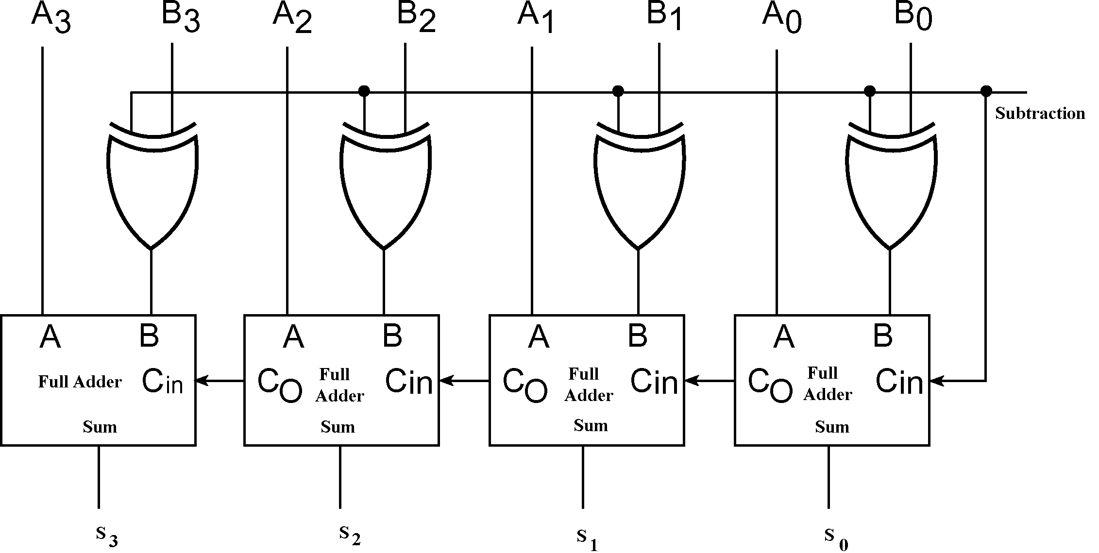
Binary Adder/Subtractor | Electronics Tutorial

